Bow and Warp Measurement of Silicon Wafers Using Confocal Sensors Posted in: Confocal Displacement Sensors – Tags: Confocal Sensors, Electronics Manufacturing, Profiling Measurement
Last Updated: March 20, 2023
Silicon wafers are the base materials for integrated circuits, the building blocks of microelectronics used in many computers, cell phones and other devices. And while used for a variety of common items, making and measuring silicon wafers is a complicated and exacting process.
In the production of silicon wafers, manufacturers are particularly concerned with bow, warp and overall flatness of the substrates. Bow measurement is the deviation from the center point of the median surface. The location of the median surface must be known in order to make highly accurate measurements. Bow can be a positive or a negative number depending on whether the center point is above or below the reference plane.
Warp measurement is the difference between the maximum and minimum distances of the median surface using the entire median surface rather than just the center point as with bow measurements. Warp wafers measurements are determined by factors such as the wafer diameter, the wafer thickness, gravity, and how the wafer is held.
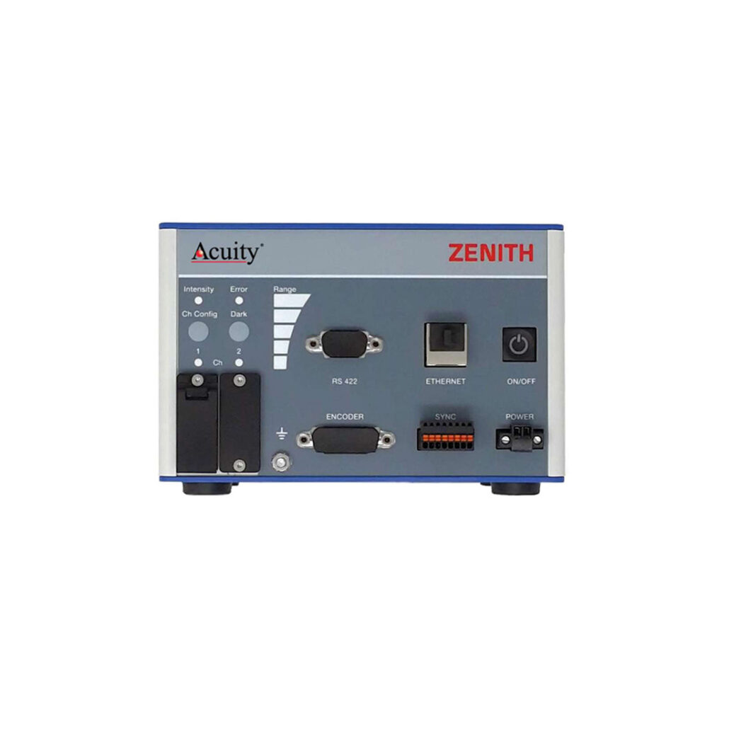
Wafer manufacturers use confocal sensors in their custom inspection systems to precisely measure the 2D flatness profile of each wafer. They then use this data to calculate bow and warp parameters. Acuity confocal sensors measure well on polished, mirror-like surfaces with little noise.
Related Products
Sarah has been our technical support and sales engineer for 5+ years. If you've ever reached out to Acuity Laser for tech support, more than likely, Sarah is the one who helped you.


